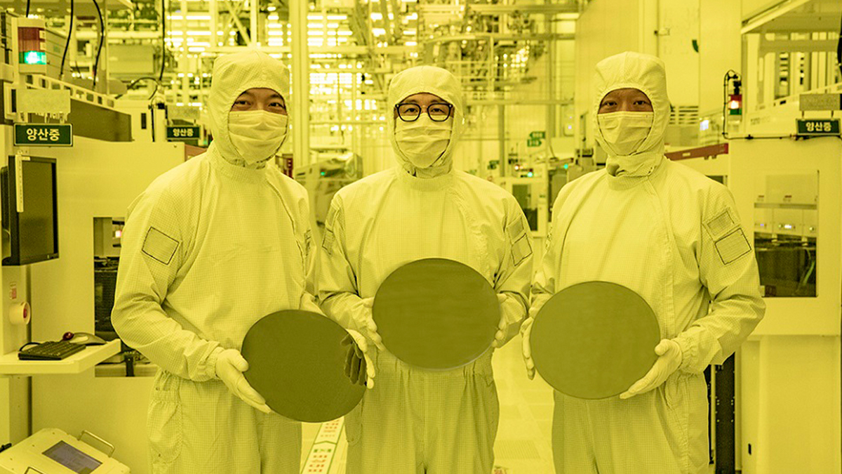
Samsung Begins Production Of World’s First 3nm Chips
Today, Samsung Electronics revealed that production of its 3-nanometer (nm) manufacturing node using the Gate-All-Around (GAA) transistor architecture has begun.
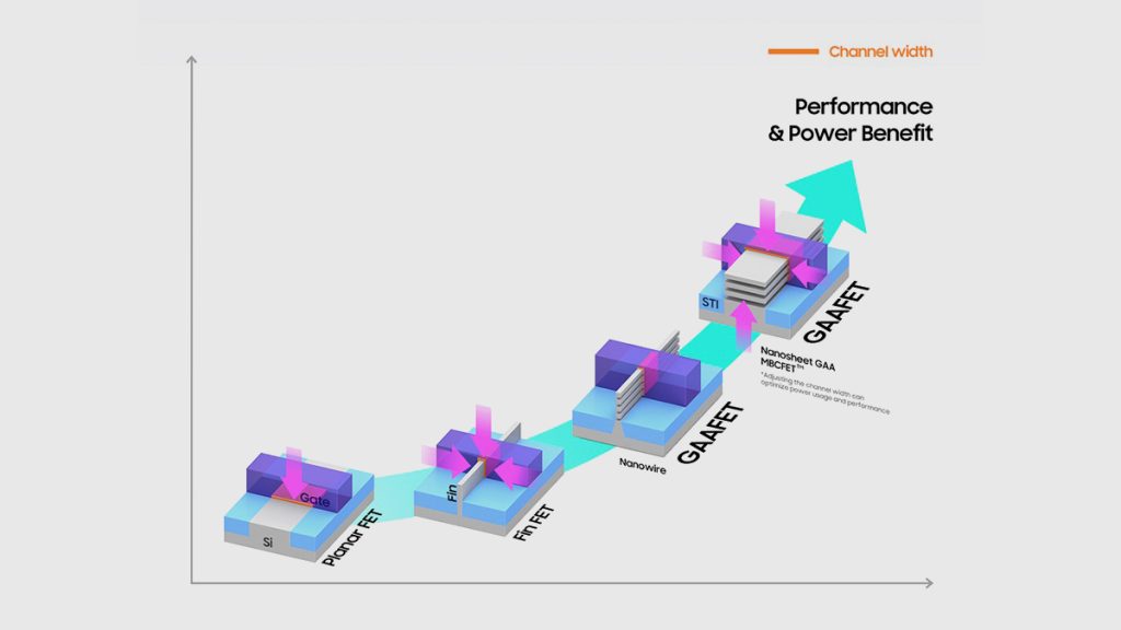
The company said that when matched to its 5nm process, their 3nm process consumes 45% less power, offers improved performance by 23%, and has a 16% smaller surface area. Samsung’s 3nm process node incorporates a gate-all-around (GAA) transistor architecture that packs larger channels in gates for electricity to flow through while lowering the voltage level compared to the preceding FinFET transistor architecture.
As the term implies, the gates completely enclose the channels in GAA, and the fact that all four sides of the channels are utilized enables a greater amount of drive current to pass through the gates in comparison to FinFET, which only employs three of the sides of the channels.
The firm also talked about the adaptability of the design of its 3nm process node, which allowed it to modify the channel width to provide the utmost satisfaction to its clientele. Samsung said that they were also working on a second-generation 3nm process node that would be better in terms of power use, performance, and surface area.
Memory chip production is Samsung’s speciality; the company is the world’s second-biggest foundry and the largest contract chipmaker. It’s really contending with the largest foundry in the industry, Taiwan Semiconductor Manufacturing Company (TSMC), to adopt more advanced process nodes before it does so. TSMC is getting ready to commence mass production using its own 3nm process node. According to Samsung, the chips that are presently being manufactured using its first 3nm process node are for a high-performance, low-power computing application.
To assist customers in achieving a higher level of product perfection in a shorter amount of time, Samsung Electronics began offering a tried-and-true design infrastructure in the third quarter of 2021. This was possible because Samsung Advanced Foundry Ecosystem (SAFE) partners like Ansys, Cadence, Siemens, and Synopsys did a lot of work to get ready.
The company aims to broaden the applicability of the node to mobile CPUs in the future, though. The company didn’t reveal which client it was now manufacturing 3nm chips in mass quantities for. The most recent 3nm battle between the two companies will come down to whoever can secure more orders from large clients, like Qualcomm, for mobile CPUs that will be used in flagship devices in the next year.
Speaking of the commencement, Dr. Siyoung Choi, President and Head of Foundry Business at Samsung Electronics, said,
Samsung has grown rapidly as we continue to demonstrate leadership in applying next-generation technologies to manufacturing, such as foundry industry’s first High-K Metal Gate, FinFET, as well as EUV. We seek to continue this leadership with the world’s first 3nm process with the MBCFET. We will continue active innovation in competitive technology development and build processes that help expedite achieving maturity of technology.